| The ebook FEEE - Fundamentals of Electrical Engineering and Electronics is based on material originally written by T.R. Kuphaldt and various co-authors. For more information please read the copyright pages. |

|
Home  Semiconductors Bipolar Junction Transistors The common-base amplifier Semiconductors Bipolar Junction Transistors The common-base amplifier |
||||


|
  |
|||
|
The common-base amplifier
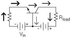
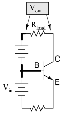
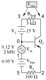
It is called the common-base configuration because (DC power source aside), the signal source and the load share the base of the transistor as a common connection point:
Perhaps the most striking characteristic of this configuration is that the input signal source must carry the full emitter current of the transistor, as indicated by the heavy arrows in the first illustration. As we know, the emitter current is greater than any other current in the transistor, being the sum of base and collector currents. In the last two amplifier configurations, the signal source was connected to the base lead of the transistor, thus handling the least current possible. Because the input current exceeds all other currents in the circuit, including the output current, the current gain of this amplifier is actually less than 1 (notice how Rload is connected to the collector, thus carrying slightly less current than the signal source). In other words, it attenuates current rather than amplifying it. With common-emitter and common-collector amplifier configurations, the transistor parameter most closely associated with gain was β. In the common-base circuit, we follow another basic transistor parameter: the ratio between collector current and emitter current, which is a fraction always less than 1. This fractional value for any transistor is called the alpha ratio, or α ratio. Since it obviously can't boost signal current, it only seems reasonable to expect it to boost signal voltage. A SPICE simulation will vindicate that assumption:
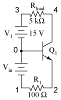
common-base amplifier
vin 0 1
r1 1 2 100
q1 4 0 2 mod1
v1 3 0 dc 15
rload 3 4 5k
.model mod1 npn
.dc vin 0.6 1.2 .02
.plot dc v(3,4)
.end
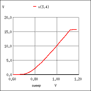
Notice how in this simulation the output voltage goes from practically nothing (cutoff) to 15.75 volts (saturation) with the input voltage being swept over a range of 0.6 volts to 1.2 volts. In fact, the output voltage plot doesn't show a rise until about 0.7 volts at the input, and cuts off (flattens) at about 1.12 volts input. This represents a rather large voltage gain with an output voltage span of 15.75 volts and an input voltage span of only 0.42 volts: a gain ratio of 37.5, or 31.48 dB. Notice also how the output voltage (measured across Rload) actually exceeds the power supply (15 volts) at saturation, due to the series-aiding effect of the the input voltage source. A second set of SPICE analyses with an AC signal source (and DC bias voltage) tells the same story: a high voltage gain.
common-base amplifier
vin 0 1 sin (0 0.12 2000 0 0)
vbias 1 5 dc 0.95
r1 5 2 100
q1 4 0 2 mod1
v1 3 0 dc 15
rload 3 4 5k
.model mod1 npn
.tran 0.02m 0.78m
.plot tran v(1,0) v(4,3)
.end
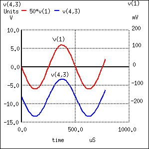
As you can see, the input and output waveforms are in phase with each other. This tells us that the common-base amplifier is non-inverting.
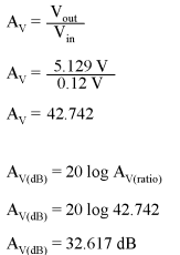
common-base amplifier
vin 0 1 ac 0.12
vbias 1 5 dc 0.95
r1 5 2 100
q1 4 0 2 mod1
v1 3 0 dc 15
rload 3 4 5k
.model mod1 npn
.ac lin 1 2000 2000
.print ac v(1,0) v(3,4)
.end


freq          v(1)        v(3,4)
2.000E+03     1.200E-01   5.129E+00
Voltage figures from the second analysis (AC mode) show a voltage gain of 42.742 (5.129 V / 0.12 V), or 32.617 dB:
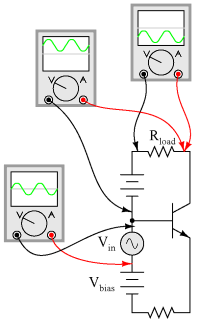
Here's another view of the circuit, showing the phase relations and DC offsets of various signals in the circuit just simulated:
. . . and for a PNP transistor:
Predicting voltage gain for the common-base amplifier configuration is quite difficult, and involves approximations of transistor behavior that are difficult to measure directly. Unlike the other amplifier configurations, where voltage gain was either set by the ratio of two resistors (common-emitter), or fixed at an unchangeable value (common-collector), the voltage gain of the common-base amplifier depends largely on the amount of DC bias on the input signal. As it turns out, the internal transistor resistance between emitter and base plays a major role in determining voltage gain, and this resistance changes with different levels of current through the emitter. While this phenomenon is difficult to explain, it is rather easy to demonstrate through the use of computer simulation. What I'm going to do here is run several SPICE simulations on a common-base amplifier circuit, changing the DC bias voltage slightly while keeping the AC signal amplitude and all other circuit parameters constant. As the voltage gain changes from one simulation to another, different output voltage amplitudes will be noticed as a result. Although these analyses will all be conducted in the AC mode, they were first "proofed" in the transient analysis mode (voltage plotted over time) to ensure that the entire wave was being faithfully reproduced and not "clipped" due to improper biasing. No meaningful calculations of gain can be based on waveforms that are distorted:
common-base amplifier DC bias = 0.85 volts
vin 0 1 ac 0.08
vbias 1 5 dc 0.85
r1 5 2 100
q1 4 0 2 mod1
v1 3 0 dc 15
rload 3 4 5k
.model mod1 npn
.ac lin 1 2000 2000
.print ac v(1,0) v(3,4)
.end


freq          v(1)        v(3,4)
2.000E+03     8.000E-02   3.005E+00
common-base amplifier dc bias = 0.9 volts
vin 0 1 ac 0.08
vbias 1 5 dc 0.90
r1 5 2 100
q1 4 0 2 mod1
v1 3 0 dc 15
rload 3 4 5k
.model mod1 npn
.ac lin 1 2000 2000
.print ac v(1,0) v(3,4)
.end


freq          v(1)        v(3,4)
2.000E+03     8.000E-02   3.264E+00
common-base amplifier dc bias = 0.95 volts
vin 0 1 ac 0.08
vbias 1 5 dc 0.95
r1 5 2 100
q1 4 0 2 mod1
v1 3 0 dc 15
rload 3 4 5k
.model mod1 npn
.ac lin 1 2000 2000
.print ac v(1,0) v(3,4)
.end


freq          v(1)        v(3,4)
2.000E+03     8.000E-02   3.419E+00
A trend should be evident here: with increases in DC bias voltage, voltage gain increases as well. We can see that the voltage gain is increasing because each subsequent simulation produces greater output voltage for the exact same input signal voltage (0.08 volts). As you can see, the changes are quite large, and they are caused by miniscule variations in bias voltage! The combination of very low current gain (always less than 1) and somewhat unpredictable voltage gain conspire against the common-base design, relegating it to few practical applications.
|
||||
| Home Semiconductors Bipolar Junction Transistors The common-base amplifier |
|
|||

Last Update: 2010-12-01