| The ebook FEEE - Fundamentals of Electrical Engineering and Electronics is based on material originally written by T.R. Kuphaldt and various co-authors. For more information please read the copyright pages. |
|
Home  Semiconductors Operational Amplifiers Practical Considerations Common-Mode Gain Semiconductors Operational Amplifiers Practical Considerations Common-Mode Gain |
|


|
  |
|
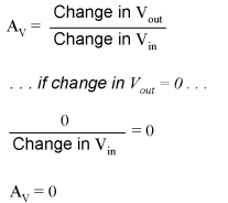
Common-Mode GainAs stated before, an ideal differential amplifier only amplifies the voltage difference between its two inputs. If the two inputs of a differential amplifier were to be shorted together (thus ensuring zero potential difference between them), there should be no change in output voltage for any amount of voltage applied between those two shorted inputs and ground:
Voltage that is common between either of the inputs and ground, as "Vcommon-mode" is in this case, is called common-mode voltage. As we vary this common voltage, the perfect differential amplifier's output voltage should hold absolutely steady (no change in output for any arbitrary change in common-mode input). This translates to a common-mode voltage gain of zero.
The operational amplifier, being a differential amplifier with high differential gain, would ideally have zero common-mode gain as well. In real life, however, this is not easily attained. Thus, common-mode voltages will invariably have some effect on the op-amp's output voltage. Common-mode rejection ratio CMRRThe performance of a real op-amp in this regard is most commonly measured in terms of its differential voltage gain (how much it amplifies the difference between two input voltages) versus its common-mode voltage gain (how much it amplifies a common-mode voltage). The ratio of the former to the latter is called the common-mode rejection ratio, abbreviated as CMRR:
An ideal op-amp, with zero common-mode gain would have an infinite CMRR. Real op-amps have high CMRRs, the ubiquitous 741 having something around 70 dB, which works out to a little over 3,000 in terms of a ratio. Because the common mode rejection ratio in a typical op-amp is so high, common-mode gain is usually not a great concern in circuits where the op-amp is being used with negative feedback. If the common-mode input voltage of an amplifier circuit were to suddenly change, thus producing a corresponding change in the output due to common-mode gain, that change in output would be quickly corrected as negative feedback and differential gain (being much greater than common-mode gain) worked to bring the system back to equilibrium. Sure enough, a change might be seen at the output, but it would be a lot smaller than what you might expect. A consideration to keep in mind, though, is common-mode gain in differential op-amp circuits such as instrumentation amplifiers. Outside of the op-amp's sealed package and extremely high differential gain, we may find common-mode gain introduced by an imbalance of resistor values. To demonstrate this, we'll run a SPICE analysis on an instrumentation amplifier with inputs shorted together (no differential voltage), imposing a common-mode voltage to see what happens. First, we'll run the analysis showing the output voltage of a perfectly balanced circuit. We should expect to see no change in output voltage as the common-mode voltage changes:
instrumentation amplifier
v1 1 0
rin1 1 0 9e12
rjump 1 4 1e-12
rin2 4 0 9e12
e1 3 0 1 2 999k
e2 6 0 4 5 999k
e3 9 0 8 7 999k
rload 9 0 10k
r1 2 3 10k
rgain 2 5 10k
r2 5 6 10k
r3 3 7 10k
r4 7 9 10k
r5 6 8 10k
r6 8 0 10k
.dc v1 0 10 1
.print dc v(9)
.end


v1            v(9)
0.000E+00     0.000E+00
1.000E+00     1.355E-16
2.000E+00     2.710E-16
3.000E+00     0.000E+00   As you can see, the output voltage v(9)
4.000E+00     5.421E-16   hardly changes at all for a common-mode
5.000E+00     0.000E+00   input voltage (v1) that sweeps from 0
6.000E+00     0.000E+00   to 10 volts.
7.000E+00     0.000E+00
8.000E+00     1.084E-15
9.000E+00    -1.084E-15
1.000E+01     0.000E+00
Aside from very small deviations (actually due to quirks of SPICE rather than real behavior of the circuit), the output remains stable where it should be: at 0 volts, with zero input voltage differential. However, let's introduce a resistor imbalance in the circuit, increasing the value of R5 from 10,000 Ω to 10,500 Ω, and see what happens (the netlist has been omitted for brevity -- the only thing altered is the value of R5):
v1           v(9)
0.000E+00     0.000E+00
1.000E+00    -2.439E-02
2.000E+00    -4.878E-02
3.000E+00    -7.317E-02   This time we see a significant variation
4.000E+00    -9.756E-02   (from 0 to 0.2439 volts) in output voltage
5.000E+00    -1.220E-01   as the common-mode input voltage sweeps
6.000E+00    -1.463E-01   from 0 to 10 volts as it did before.
7.000E+00    -1.707E-01
8.000E+00    -1.951E-01
9.000E+00    -2.195E-01
1.000E+01    -2.439E-01
Our input voltage differential is still zero volts, yet the output voltage changes significantly as the common-mode voltage is changed. This is indicative of a common-mode gain, something we're trying to avoid. More than that, it's a common-mode gain of our own making, having nothing to do with imperfections in the op-amps themselves. With a much-tempered differential gain (actually equal to 3 in this particular circuit) and no negative feedback outside the circuit, this common-mode gain will go unchecked in an instrument signal application. There is only one way to correct this common-mode gain, and that is to balance all the resistor values. When designing an instrumentation amplifier from discrete components (rather than purchasing one in an integrated package), it is wise to provide some means of making fine adjustments to at least one of the four resistors connected to the final op-amp to be able to "trim away" any such common-mode gain. Providing the means to "trim" the resistor network has additional benefits as well. Suppose that all resistor values are exactly as they should be, but a common-mode gain exists due to an imperfection in one of the op-amps. With the adjustment provision, the resistance could be trimmed to compensate for this unwanted gain. Latch-upOne quirk of some op-amp models is that of output latch-up, usually caused by the common-mode input voltage exceeding allowable limits. If the common-mode voltage falls outside of the manufacturer's specified limits, the output may suddenly "latch" in the high mode (saturate at full output voltage). In JFET-input operational amplifiers, latch-up may occur if the common-mode input voltage approaches too closely to the negative power supply rail voltage. On the TL082 op-amp, for example, this occurs when the common-mode input voltage comes within about 0.7 volts of the negative power supply rail voltage. Such a situation may easily occur in a single-supply circuit, where the negative power supply rail is ground (0 volts), and the input signal is free to swing to 0 volts. Latch-up may also be triggered by the common-mode input voltage exceeding power supply rail voltages, negative or positive. As a rule, you should never allow either input voltage to rise above the positive power supply rail voltage, or sink below the negative power supply rail voltage, even if the op-amp in question is protected against latch-up (as are the 741 and 1458 op-amp models). At the very least, the op-amp's behavior may become unpredictable. At worst, the kind of latch-up triggered by input voltages exceeding power supply voltages may be destructive to the op-amp. While this problem may seem easy to avoid, its possibility is more likely than you might think. Consider the case of an operational amplifier circuit during power-up. If the circuit receives full input signal voltage before its own power supply has had time enough to charge the filter capacitors, the common-mode input voltage may easily exceed the power supply rail voltages for a short time. If the op-amp receives signal voltage from a circuit supplied by a different power source, and its own power source fails, the signal voltage(s) may exceed the power supply rail voltages for an indefinite amount of time!
|
|
| Home Semiconductors Operational Amplifiers Practical Considerations Common-Mode Gain |
|


Last Update: 2010-12-01