| The ebook FEEE - Fundamentals of Electrical Engineering and Electronics is based on material originally written by T.R. Kuphaldt and various co-authors. For more information please read the copyright pages. |
|
Home  Semiconductors Junction Field-Effect Transistors Introduction Semiconductors Junction Field-Effect Transistors Introduction |
|


|
  |
|
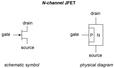
IntroductionA transistor is a linear semiconductor device that controls current with the application of a lower-power electrical signal. Transistors may be roughly grouped into two major divisions: bipolar and field-effect. In the last chapter we studied bipolar transistors, which utilize a small current to control a large current. In this chapter, we'll introduce the general concept of the field-effect transistor -- a device utilizing a small voltage to control current -- and then focus on one particular type: the junction field-effect transistor. In the next chapter we'll explore another type of field-effect transistor, the insulated gate variety. All field-effect transistors are unipolar rather than bipolar devices. That is, the main current through them is comprised either of electrons through an N-type semiconductor or holes through a P-type semiconductor. This becomes more evident when a physical diagram of the device is seen:
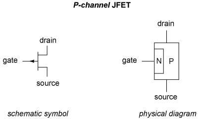
In a junction field-effect transistor, or JFET, the controlled current passes from source to drain, or from drain to source as the case may be. The controlling voltage is applied between the gate and source. Note how the current does not have to cross through a PN junction on its way between source and drain: the path (called a channel) is an uninterrupted block of semiconductor material. In the image just shown, this channel is an N-type semiconductor. P-type channel JFETs are also manufactured:
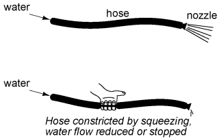
Generally, N-channel JFETs are more commonly used than P-channel. The reasons for this have to do with obscure details of semiconductor theory, which I'd rather not discuss in this chapter. As with bipolar transistors, I believe the best way to introduce field-effect transistor usage is to avoid theory whenever possible and concentrate instead on operational characteristics. The only practical difference between N- and P-channel JFETs you need to concern yourself with now is biasing of the PN junction formed between the gate material and the channel. With no voltage applied between gate and source, the channel is a wide-open path for electrons to flow. However, if a voltage is applied between gate and source of such polarity that it reverse-biases the PN junction, the flow between source and drain connections becomes limited, or regulated, just as it was for bipolar transistors with a set amount of base current. Maximum gate-source voltage "pinches off" all current through source and drain, thus forcing the JFET into cutoff mode. This behavior is due to the depletion region of the PN junction expanding under the influence of a reverse-bias voltage, eventually occupying the entire width of the channel if the voltage is great enough. This action may be likened to reducing the flow of a liquid through a flexible hose by squeezing it: with enough force, the hose will be constricted enough to completely block the flow.
Note how this operational behavior is exactly opposite of the bipolar junction transistor. Bipolar transistors are normally-off devices: no current through the base, no current through the collector or the emitter. JFETs, on the other hand, are normally-on devices: no voltage applied to the gate allows maximum current through the source and drain. Also take note that the amount of current allowed through a JFET is determined by a voltage signal rather than a current signal as with bipolar transistors. In fact, with the gate-source PN junction reverse-biased, there should be nearly zero current through the gate connection. For this reason, we classify the JFET as a voltage-controlled device, and the bipolar transistor as a current-controlled device. If the gate-source PN junction is forward-biased with a small voltage, the JFET channel will "open" a little more to allow greater currents through. However, the PN junction of a JFET is not built to handle any substantial current itself, and thus it is not recommended to forward-bias the junction under any circumstances. This is a very condensed overview of JFET operation. In the next section, we'll explore the use of the JFET as a switching device.
|
|
| Home Semiconductors Junction Field-Effect Transistors Introduction |
|
Last Update: 2010-11-19