| The ebook FEEE - Fundamentals of Electrical Engineering and Electronics is based on material originally written by T.R. Kuphaldt and various co-authors. For more information please read the copyright pages. |

|
Home  Semiconductors Operational Amplifiers Practical Considerations Bias Current Semiconductors Operational Amplifiers Practical Considerations Bias Current |
|||


|
  |
||
|
Bias CurrentBias current, op-ampInputs on an op-amp have extremely high input impedances. That is, the input currents entering or exiting an op-amp's two input signal connections are extremely small. For most purposes of op-amp circuit analysis, we treat them as though they don't exist at all. We analyze the circuit as though there was absolutely zero current entering or exiting the input connections. This idyllic picture, however, is not entirely true. Op-amps, especially those op-amps with bipolar transistor inputs, have to have some amount of current through their input connections in order for their internal circuits to be properly biased. These currents, logically, are called bias currents. Under certain conditions, op-amp bias currents may be problematic. The following circuit illustrates one of those problem conditions:
At first glance, we see no apparent problems with this circuit. A thermocouple, generating a small voltage proportional to temperature (actually, a voltage proportional to the difference in temperature between the measurement junction and the "reference" junction formed when the alloy thermocouple wires connect with the copper wires leading to the op-amp) drives the op-amp either positive or negative. In other words, this is a kind of comparator circuit, comparing the temperature between the end thermocouple junction and the reference junction (near the op-amp). The problem is this: the wire loop formed by the thermocouple does not provide a path for both input bias currents, because both bias currents are trying to go the same way (either into the op-amp or out of it).
In order for this circuit to work properly, we must ground one of the input wires, thus providing a path to (or from) ground for both currents:
Not necessarily an obvious problem, but a very real one! Another way input bias currents may cause trouble is by dropping unwanted voltages across circuit resistances. Take this circuit for example:
We expect a voltage follower circuit such as the one above to reproduce the input voltage precisely at the output. But what about the resistance in series with the input voltage source? If there is any bias current through the noninverting (+) input at all, it will drop some voltage across Rin, thus making the voltage at the noninverting input unequal to the actual Vin value. Bias currents are usually in the microamp range, so the voltage drop across Rin won't be very much, unless Rin is very large. One example of an application where the input resistance (Rin) would be very large is that of pH probe electrodes, where one electrode contains an ion-permeable glass barrier (a very poor conductor, with millions of Ω of resistance). If we were actually building an op-amp circuit for pH electrode voltage measurement, we'd probably want to use a FET or MOSFET (IGFET) input op-amp instead of one built with bipolar transistors (for less input bias current). But even then, what slight bias currents may remain can cause measurement errors to occur, so we have to find some way to mitigate them through good design. One way to do so is based on the assumption that the two input bias currents will be the same. In reality, they are often close to being the same, the difference between them referred to as the input offset current. If they are the same, then we should be able to cancel out the effects of input resistance voltage drop by inserting an equal amount of resistance in series with the other input, like this:
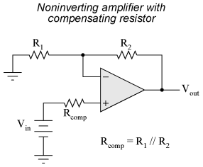
With the additional resistance added to the circuit, the output voltage will be closer to Vin than before, even if there is some offset between the two input currents. For both inverting and noninverting amplifier circuits, the bias current compensating resistor is placed in series with the noninverting (+) input to compensate for bias current voltage drops in the divider network:
In either case, the compensating resistor value is determined by calculating the parallel resistance value of R1 and R2. Why is the value equal to the parallel equivalent of R1 and R2? When using the Superposition Theorem to figure how much voltage drop will be produced by the inverting (-) input's bias current, we treat the bias current as though it were coming from a current source inside the op-amp and short-circuit all voltage sources (Vin and Vout). This gives two parallel paths for bias current (through R1 and through R2, both to ground). We want to duplicate the bias current's effect on the noninverting (+) input, so the resistor value we choose to insert in series with that input needs to be equal to R1 in parallel with R2. A related problem, occasionally experienced by students just learning to build operational amplifier circuits, is caused by a lack of a common ground connection to the power supply. It is imperative to proper op-amp function that some terminal of the DC power supply be common to the "ground" connection of the input signal(s). This provides a complete path for the bias currents, feedback current(s), and for the load (output) current. Take this circuit illustration, for instance, showing a properly grounded power supply:
Here, arrows denote the path of electron flow through the power supply batteries, both for powering the op-amp's internal circuitry (the "potentiometer" inside of it that controls output voltage), and for powering the feedback loop of resistors R1 and R2. Suppose, however, that the ground connection for this "split" DC power supply were to be removed. The effect of doing this is profound:
No electrons may flow in or out of the op-amp's output terminal, because the pathway to the power supply is a "dead end." Thus, no electrons flow through the ground connection to the left of R1, neither through the feedback loop. This effectively renders the op-amp useless: it can neither sustain current through the feedback loop, nor through a grounded load, since there is no connection from any point of the power supply to ground. The bias currents are also stopped, because they rely on a path to the power supply and back to the input source through ground. The following diagram shows the bias currents (only), as they go through the input terminals of the op-amp, through the base terminals of the input transistors, and eventually through the power supply terminal(s) and back to ground.
Without a ground reference on the power supply, the bias currents will have no complete path for a circuit, and they will halt. Since bipolar junction transistors are current-controlled devices, this renders the input stage of the op-amp useless as well, as both input transistors will be forced into cutoff by the complete lack of base current.
|
|||
| Home Semiconductors Operational Amplifiers Practical Considerations Bias Current |
|
||


Last Update: 2010-12-01