| Transistor Basics is a free introductory textbook on transistors and their basic applications. See the editorial for more information.... |
|
Home  Transistors and Their Operation Junction Transistors Construction and Operation Transistors and Their Operation Junction Transistors Construction and Operation |
||


|
  |
|
|
Construction and Operation of Junction TransistorsAuthor: Leonard Krugman In Chapter 1, it was observed that a combination of P- and N-type germanium form a P-N junction. In effect, this combination produces a germanium diode. The germanium diode has been incorporated in television circuits for several years to serve as second detectors, and has been used in other circuits where its excellent rectifying characteristic is useful. Consider now the effect of combining two germanium diodes into one unit and, for further simplification, make the P-type section common to both. This new device, illustrated by Fig. 2-5, is the basic N-P-N junction transistor. In actual construction, the P section is very narrow as compared to the strips of N-type germanium. As will be seen later, the narrow middle section is required for proper transistor operation.
Fig, 2-5. Construction of basic N-P-N junction transistor. Courtesy CBS-Hytron.
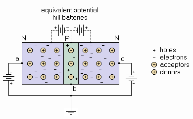
Although the junction transistor is a physical combination of two germanium diodes, conduction in the transistor is decidedly different from that in the diode or point-contact transistor. Observe that in Fig. 2-6 the negative potential at the emitter electrode pushes the free electrons towards the P-N junction. At the junction, as discussed in Chapter 1, a potential hill is set up by the action of the fixed donor and acceptor atoms. Since the emitter battery acts to flatten this emitter-base potential hill, a number of electrons pass this barrier and enter the P base region. The number of electrons crossing the barrier is proportional to the value of emitter battery potential. Some of these electrons combine with holes in the P base region, but most pass through and enter the N collector region. The loss of electrons in the P base region remains low (approximately five percent) because: (1) the base section is thin, and (2) the potential hill at the collector-base junction acts to accelerate the electrons into the N collector region. In the N region, the electrons are attracted to the positive collector.
Fig. 2-6. Basic N-P-N transistor.
|
||
| Home Transistors and Their Operation Junction Transistors Construction and Operation |
|
|

Last Update: 2010-11-17