| Transistor Basics is a free introductory textbook on transistors and their basic applications. See the editorial for more information.... |

|
Home  Transistors and Their Operation Transistor Tetrode Transistors and Their Operation Transistor Tetrode |
||


|
  |
|
|
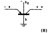
Transistor TetrodeAuthor: Leonard Krugman The frequency response of the conventional junction transistor is limited by several factors. First, the frequency cutoff (the frequency at which the current gain drops sharply) is inversely proportional to both the base resistance and to the square of the thickness of the junction layer. In addition, the frequency cutoff is also inversely proportional to the collector junction capacitance, considered only at high frequencies. Figures 2-11 (A) and 2-11 (B) illustrate the structural and symbolic representations of the junction transistor tetrode.
Fig. 2-11. Tetrode junction transistor: (A) structural representation, (B) symbolic representation.
For proper operation, the second base electrode is biased to about -6 volts with respect to the base. The resulting bias current is approximately one milliampere. In a typical case this bias reduces the base resistance from 1,000 to 40 ohms; the change in emitter resistance is negligible. The current gain is reduced from .95 to .75, and the collector resistance is reduced from 3.0 to 1.5 megohms. The frequency response cutoff is increased from 0.5 to 5 megacycles. Thus, an increased bandwidth is obtained at the expense of lower available gain. The effect of the junction area thickness is decreased by using very thin P layers (roughly .0005 inch). The collector junction capacitance is reduced by decreasing the collector junction area.
|
||
| Home Transistors and Their Operation Transistor Tetrode |
|
|

Last Update: 2007-09-13