| Transistor Basics is a free introductory textbook on transistors and their basic applications. See the editorial for more information.... |

|
Home  Transistor Amplifiers Class B Transistor Amplifiers Push-Pull Circuitry Transistor Amplifiers Class B Transistor Amplifiers Push-Pull Circuitry |
||


|
  |
|
|
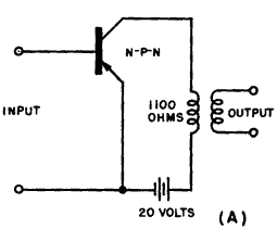
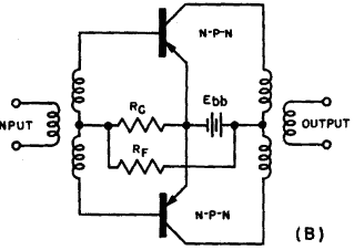
Push-Pull CircuitryAuthor: Leonard Krugman Two Class B amplifiers connected as a push-pull stage, using two of the circuits illustrated in Fig. 5-12 (A), will not operate. One transistor will always be biased in the reverse direction by the input signal, thereby causing its input resistance to become very high. This condition can be eliminated by using a center-tapped input transformer and connecting the center tap to the common emitter electrodes. This circuit is characterized by a distorted output wave. The distortion is particularly evident when the signal generator resistance is low. However, the distortion can be reduced within limits by introducing base bias into the circuit.
Fig. 5-12. (A) Class B circuit (constant voltage). (B) Class B push-pull operation.
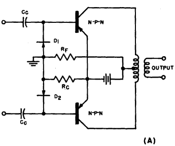
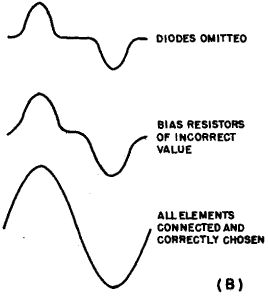
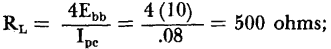
Fig. 5-13. (A) Class & push-pull operation without input transformer. (b) Output waveforms. Another arrangement for a transistor push-pull Class B stage is illustrated in Fig. 5-13(A). This circuit permits the elimination of the input transformers. The diodes D1 and D2 prevent each transistor from cutting off when it is biased in the negative (reverse bias) direction by the input signal, since the diodes effectively short out the signal-induced bias. The point at which this bypass action occurs is determined by the bias due to resistors RF and Rc. These resistors also furnish base bias to the transistors to minimize cross-over distortion. Figure 5-13 (B) illustrates the effect of diodes and bias resistors on distortion of the output signal. The detailed operating characteristics of a Class B transistor push-pull amplifier are determined by the same methods used in similar vacuum tube circuits. The approximate values of the major characteristics can be calculated as illustrated in the following example: Assume that the transistors to be used in the Class B push-pull circuit have a maximum collector dissipation rating of 100 milliwatts, and assume that a battery Ebb = 10 volts is specified. The collector dissipation Pc in each transistor is approximately Then The required load for maximum power output is: and the power output is approximately
|
||
| Home Transistor Amplifiers Class B Transistor Amplifiers Push-Pull Circuitry |
|
|
 where Ipc is the peak collector current.
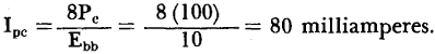
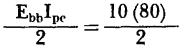 = 400 milliwatts, or four times the maximum collector dissipation of each transistor.
Last Update: 2010-11-17