| Transistor Basics is a free introductory textbook on transistors and their basic applications. See the editorial for more information.... |

|
Home  Transistor High Frequency Applications The Transistor at High Frequencies Transit Time, Dispersion Effect Transistor High Frequency Applications The Transistor at High Frequencies Transit Time, Dispersion Effect |
||


|
  |
|
|
Transit Time, Dispersion EffectAuthor: Leonard Krugman In the earlier chapters it was noted that the low-frequency, small-signal parameters change as the operating frequency is increased appreciably above the audio range. Figure 7-1 illustrates the low-frequency equivalent circuit of the transistor including the collector junction capacitance Cc. At higher frequencies this equivalent circuit must be modified to include the effects of the current carriers' transit time on the transistor parameters. The transit time of the carriers (holes or electrons) is one of the major factors limiting the high frequency response of the transistor.
Fig. 7-1. Low-frequency equivalent circuit of the transistor (including collector junction capacitance).
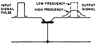
 . The degradation in frequency response becomes steadily worse as the operating frequency is increased, until eventually there is no relationship between the input and output waveforms (and no gain). . The degradation in frequency response becomes steadily worse as the operating frequency is increased, until eventually there is no relationship between the input and output waveforms (and no gain).
Fig. 7-2. Transistor high-frequency dispersion effect. Another factor that limits the high frequency response of the transistor is the capacitive reactance of the emitter input circuit, which behaves as if re is shunted by a capacitor. This reactive parameter is reduced if the source impedance is made as low as possible. Since rb is also effectively in series with the source, a good high frequency transistor must have a low base resistance. If the source impedance and base resistance are low, the upper frequency response limit is determined primarily by the collector junction capacitance and the variation in the current gain.
|
||
| Home Transistor High Frequency Applications The Transistor at High Frequencies Transit Time, Dispersion Effect |
|
|

Last Update: 2010-11-17