| The ebook FEEE - Fundamentals of Electrical Engineering and Electronics is based on material originally written by T.R. Kuphaldt and various co-authors. For more information please read the copyright pages. |

|
Home  Semiconductors Bipolar Junction Transistors Practical Biasing techniques Semiconductors Bipolar Junction Transistors Practical Biasing techniques |
|||
| See also: Biasing techniques | |||


|
  |
||
|
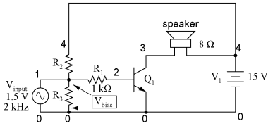
Practical Biasing TechniquesNow that we know a little more about the consequences of different DC bias voltage levels, it is time to investigate practical biasing techniques. So far, I've shown a small DC voltage source (battery) connected in series with the AC input signal to bias the amplifier for whatever desired class of operation. In real life, the connection of a precisely-calibrated battery to the input of an amplifier is simply not practical. Even if it were possible to customize a battery to produce just the right amount of voltage for any given bias requirement, that battery would not remain at its manufactured voltage indefinitely. Once it started to discharge and its output voltage drooped, the amplifier would begin to drift in the direction of class B operation. Take this circuit, illustrated in the common-emitter section for a SPICE simulation, for instance:
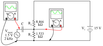
That 2.3 volt "Vbias" battery would not be practical to include in a real amplifier circuit. A far more practical method of obtaining bias voltage for this amplifier would be to develop the necessary 2.3 volts using a voltage divider network connected across the 15 volt battery. After all, the 15 volt battery is already there by necessity, and voltage divider circuits are very easy to design and build. Let's see how this might look:
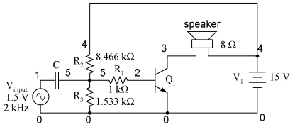
If we choose a pair of resistor values for R2 and R3 that will produce 2.3 volts across R3 from a total of 15 volts (such as 8466 Ω for R2 and 1533 Ω for R3), we should have our desired value of 2.3 volts between base and emitter for biasing with no signal input. The only problem is, this circuit configuration places the AC input signal source directly in parallel with R3 of our voltage divider. This is not acceptable, as the AC source will tend to overpower any DC voltage dropped across R3. Parallel components must have the same voltage, so if an AC voltage source is directly connected across one resistor of a DC voltage divider, the AC source will "win" and there will be no DC bias voltage added to the signal. One way to make this scheme work, although it may not be obvious why it will work, is to place a coupling capacitor between the AC voltage source and the voltage divider like this:
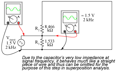
The capacitor forms a high-pass filter between the AC source and the DC voltage divider, passing almost all of the AC signal voltage on to the transistor while blocking all DC voltage from being shorted through the AC signal source. This makes much more sense if you understand the superposition theorem and how it works. According to superposition, any linear, bilateral circuit can be analyzed in a piecemeal fashion by only considering one power source at a time, then algebraically adding the effects of all power sources to find the final result. If we were to separate the capacitor and R2 With only the AC signal source in effect, and a capacitor with an arbitrarily low impedance at signal frequency, almost all the AC voltage appears across R3:
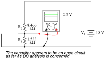
With only the DC source in effect, the capacitor appears to be an open circuit, and thus neither it nor the shorted AC signal source will have any effect on the operation of the R2
Combining these two separate analyses, we get a superposition of (almost) 1.5 volts AC and 2.3 volts DC, ready to be connected to the base of the transistor:
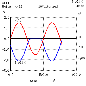
Enough talk -- it's about time for a SPICE simulation of the whole amplifier circuit. I'll use a capacitor value of 100 μF to obtain an arbitrarily low (0.796 Ω) impedance at 2000 Hz:
voltage divider biasing
vinput 1 0 sin (0 1.5 2000 0 0)
c1 1 5 100u
r1 5 2 1k
r2 4 5 8466
r3 5 0 1533
q1 3 2 0 mod1
rspkr 3 4 8
v1 4 0 dc 15
.model mod1 npn
.tran 0.02m 0.78m
.plot tran v(1,0) i(v1)
.end
Notice that there is substantial distortion in the output waveform here: the sine wave is being clipped during most of the input signal's negative half-cycle. This tells us the transistor is entering into cutoff mode when it shouldn't (I'm assuming a goal of class A operation as before). Why is this? This new biasing technique should give us exactly the same amount of DC bias voltage as before, right?
With the capacitor and R2
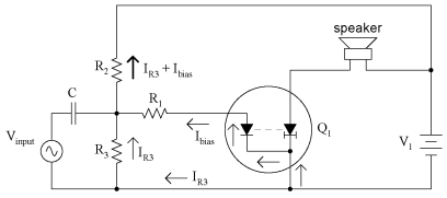
A voltage divider's output depends not only on the size of its constituent resistors, but also on how much current is being divided away from it through a load. In this case, the base-emitter PN junction of the transistor is a load that decreases the DC voltage dropped across R3, due to the fact that the bias current joins with R3's current to go through R2, upsetting the divider ratio formerly set by the resistance values of R2 and R3. In order to obtain a DC bias voltage of 2.3 volts, the values of R2 and/or R3 must be adjusted to compensate for the effect of base current loading. In this case, we want to increase the DC voltage dropped across R3, so we can lower the value of R2, raise the value of R3, or both.
voltage divider biasing
vinput 1 0 sin (0 1.5 2000 0 0)
c1 1 5 100u
r1 5 2 1k
r2 4 5 6k      <--- R2 decreased to 6 k ohms
r3 5 0 4k      <--- R3 increased to 4 k ohms
q1 3 2 0 mod1
rspkr 3 4 8
v1 4 0 dc 15
.model mod1 npn
.tran 0.02m 0.78m
.plot tran v(1,0) i(v1)
.end
As you can see, the new resistor values of 6 kΩ and 4 kΩ (R2 and R3, respectively) results in class A waveform reproduction, just the way we wanted.
|
|||
| Home Semiconductors Bipolar Junction Transistors Practical Biasing techniques |
|
||


Last Update: 2010-12-01