| The ebook FEEE - Fundamentals of Electrical Engineering and Electronics is based on material originally written by T.R. Kuphaldt and various co-authors. For more information please read the copyright pages. |

|
Home  Semiconductors Bipolar Junction Transistors Biasing techniques Semiconductors Bipolar Junction Transistors Biasing techniques |
||
| See also: Practical Biasing Techniques | ||


|
  |
|
|
Biasing techniquesIn the common-emitter section of this chapter, we saw a SPICE analysis where the output waveform resembled a half-wave rectified shape: only half of the input waveform was reproduced, with the other half being completely cut off. Since our purpose at that time was to reproduce the entire waveshape, this constituted a problem. The solution to this problem was to add a small bias voltage to the amplifier input so that the transistor stayed in active mode throughout the entire wave cycle. This addition was called a bias voltage.
Class A operation is where the entire input waveform is faithfully reproduced. Although I didn't introduce this concept back in the common-emitter section, this is what we were hoping to attain in our simulations. Class A operation can only be obtained when the transistor spends its entire time in the active mode, never reaching either cutoff or saturation. To achieve this, sufficient DC bias voltage is usually set at the level necessary to drive the transistor exactly halfway between cutoff and saturation. This way, the AC input signal will be perfectly "centered" between the amplifier's high and low signal limit levels.
Class B operation is what we had the first time an AC signal was applied to the common-emitter amplifier with no DC bias voltage. The transistor spent half its time in active mode and the other half in cutoff with the input voltage too low (or even of the wrong polarity!) to forward-bias its base-emitter junction.
By itself, an amplifier operating in class B mode is not very useful. In most circumstances, the severe distortion introduced into the waveshape by eliminating half of it would be unacceptable. However, class B operation is a useful mode of biasing if two amplifiers are operated as a push-pull pair, each amplifier handling only half of the waveform at a time:
Transistor Q1 "pushes" (drives the output voltage in a positive direction with respect to ground), while transistor Q2 "pulls" the output voltage (in a negative direction, toward 0 volts with respect to ground). Individually, each of these transistors is operating in class B mode, active only for one-half of the input waveform cycle. Together, however, they function as a team to produce an output waveform identical in shape to the input waveform. A decided advantage of the class B (push-pull) amplifier design over the class A design is greater output power capability. With a class A design, the transistor dissipates a lot of energy in the form of heat because it never stops conducting current. At all points in the wave cycle it is in the active (conducting) mode, conducting substantial current and dropping substantial voltage. This means there is substantial power dissipated by the transistor throughout the cycle. In a class B design, each transistor spends half the time in cutoff mode, where it dissipates zero power (zero current = zero power dissipation). This gives each transistor a time to "rest" and cool while the other transistor carries the burden of the load. Class A amplifiers are simpler in design, but tend to be limited to low-power signal applications for the simple reason of transistor heat dissipation. There is another class of amplifier operation known as class AB, which is somewhere between class A and class B: the transistor spends more than 50% but less than 100% of the time conducting current. If the input signal bias for an amplifier is slightly negative (opposite of the bias polarity for class A operation), the output waveform will be further "clipped" than it was with class B biasing, resulting in an operation where the transistor spends the majority of the time in cutoff mode:
At first, this scheme may seem utterly pointless. After all, how useful could an amplifier be if it clips the waveform as badly as this? If the output is used directly with no conditioning of any kind, it would indeed be of questionable utility. However, with the application of a tank circuit (parallel resonant inductor-capacitor combination) to the output, the occasional output surge produced by the amplifier can set in motion a higher-frequency oscillation maintained by the tank circuit. This may be likened to a machine where a heavy flywheel is given an occasional "kick" to keep it spinning:
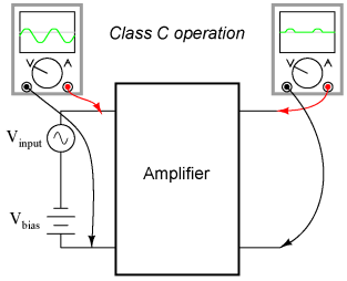
Called class C operation, this scheme also enjoys high power efficiency due to the fact that the transistor(s) spend the vast majority of time in the cutoff mode, where they dissipate zero power. The rate of output waveform decay (decreasing oscillation amplitude between "kicks" from the amplifier) is exaggerated here for the benefit of illustration. Because of the tuned tank circuit on the output, this type of circuit is usable only for amplifying signals of definite, fixed frequency. Another type of amplifier operation, significantly different from Class A, B, AB, or C, is called Class D. It is not obtained by applying a specific measure of bias voltage as are the other classes of operation, but requires a radical re-design of the amplifier circuit itself. It's a little too early in this chapter to investigate exactly how a class D amplifier is built, but not too early to discuss its basic principle of operation. A class D amplifier reproduces the profile of the input voltage waveform by generating a rapidly-pulsing squarewave output. The duty cycle of this output waveform (time "on" versus total cycle time) varies with the instantaneous amplitude of the input signal. The following plots demonstrate this principle:
The greater the instantaneous voltage of the input signal, the greater the duty cycle of the output squarewave pulse. If there can be any goal stated of the class D design, it is to avoid active-mode transistor operation. Since the output transistor of a class D amplifier is never in the active mode, only cutoff or saturated, there will be little heat energy dissipated by it. This results in very high power efficiency for the amplifier. Of course, the disadvantage of this strategy is the overwhelming presence of harmonics on the output. Fortunately, since these harmonic frequencies are typically much greater than the frequency of the input signal, they can be filtered out by a low-pass filter with relative ease, resulting in an output more closely resembling the original input signal waveform. Class D technology is typically seen where extremely high power levels and relatively low frequencies are encountered, such as in industrial inverters (devices converting DC into AC power to run motors and other large devices) and high-performance audio amplifiers. A term you will likely come across in your studies of electronics is something called quiescent, which is a modifier designating the normal, or zero input signal, condition of a circuit. Quiescent current, for example, is the amount of current in a circuit with zero input signal voltage applied. Bias voltage in a transistor circuit forces the transistor to operate at a different level of collector current with zero input signal voltage than it would without that bias voltage. Therefore, the amount of bias in an amplifier circuit determines its quiescent values. In a class A amplifier, the quiescent current should be exactly half of its saturation value (halfway between saturation and cutoff, cutoff by definition being zero). Class B and class C amplifiers have quiescent current values of zero, since they are supposed to be cutoff with no signal applied. Class AB amplifiers have very low quiescent current values, just above cutoff. To illustrate this graphically, a "load line" is sometimes plotted over a transistor's characteristic curves to illustrate its range of operation while connected to a load resistance of specific value:
A load line is a plot of collector-to-emitter voltage over a range of base currents. At the lower-right corner of the load line, voltage is at maximum and current is at zero, representing a condition of cutoff. At the upper-left corner of the line, voltage is at zero while current is at a maximum, representing a condition of saturation. Dots marking where the load line intersects the various transistor curves represent realistic operating conditions for those base currents given. Quiescent operating conditions may be shown on this type of graph in the form of a single dot along the load line. For a class A amplifier, the quiescent point will be in the middle of the load line, like this:
In this illustration, the quiescent point happens to fall on the curve representing a base current of 40 μA. If we were to change the load resistance in this circuit to a greater value, it would affect the slope of the load line, since a greater load resistance would limit the maximum collector current at saturation, but would not change the collector-emitter voltage at cutoff. Graphically, the result is a load line with a different upper-left point and the same lower-right point:
Note how the new load line doesn't intercept the 75 μA curve along its flat portion as before. This is very important to realize because the non-horizontal portion of a characteristic curve represents a condition of saturation. Having the load line intercept the 75 μA curve outside of the curve's horizontal range means that the amplifier will be saturated at that amount of base current. Increasing the load resistor value is what caused the load line to intercept the 75 μA curve at this new point, and it indicates that saturation will occur at a lesser value of base current than before. With the old, lower-value load resistor in the circuit, a base current of 75 μA would yield a proportional collector current (base current multiplied by β). In the first load line graph, a base current of 75 μA gave a collector current almost twice what was obtained at 40 μA, as the β ratio would predict. Now, however, there is only a marginal increase in collector current between base current values of 75 μA and 40 μA, because the transistor begins to lose sufficient collector-emitter voltage to continue to regulate collector current. In order to maintain linear (no-distortion) operation, transistor amplifiers shouldn't be operated at points where the transistor will saturate; that is, in any case where the load line will not potentially fall on the horizontal portion of a collector current curve. In this case, we'd have to add a few more curves to the graph before we could tell just how far we could "push" this transistor with increased base currents before it saturates.
It appears in this graph that the highest-current point on the load line falling on the straight portion of a curve is the point on the 50 μA curve. This new point should be considered the maximum allowable input signal level for class A operation. Also for class A operation, the bias should be set so that the quiescent point is halfway between this new maximum point and cutoff:
|
||
| Home Semiconductors Bipolar Junction Transistors Biasing techniques |
|
|


Last Update: 2010-12-01