| The ebook FEEE - Fundamentals of Electrical Engineering and Electronics is based on material originally written by T.R. Kuphaldt and various co-authors. For more information please read the copyright pages. |

|
Home  Digital Shift Registers Parallel-In, Parallel-Out, Universal Shift Register Digital Shift Registers Parallel-In, Parallel-Out, Universal Shift Register |
|


|
  |
|
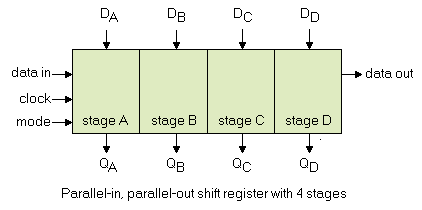
Parallel-In, Parallel-Out, Universal Shift Registerparallel-in/parallel-out universal shift register shift register, parallel-in/parallel-out universal shift registerThe purpose of the parallel-in/ parallel-out shift register is to take in parallel data, shift it, then output it as shown below. A universal shift register is a do-everything device in addition to the parallel-in/ parallel-out function.
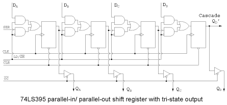
Above we apply four bit of data to a parallel-in/ parallel-out shift register at DA DB DC DD. The mode control, which may be multiple inputs, controls parallel loading vs shifting. The mode control may also control the direction of shifting in some real devices. The data will be shifted one bit position for each clock pulse. The shifted data is available at the outputs QA QB QC QD . The "data in" and "data out" are provided for cascading of multiple stages. Though, above, we can only cascade data for right shifting. We could accommodate cascading of left-shift data by adding a pair of left pointing signals, "data in" and "data out", above. The internal details of a right shifting parallel-in/ parallel-out shift register are shown below. The tri-state buffers are not strictly necessary to the parallel-in/ parallel-out shift register, but are part of the real-world device shown below. 395, 74LS395, shift register
395, 74LS395 The 74LS395 so closely matches our concept of a hypothetical right shifting parallel-in/ parallel-out shift register that we use an overly simplified version of the data sheet details above. See the link to the full data sheet more more details, later in this chapter. LD/SH' controls the AND-OR multiplexer at the data input to the FF's. If LD/SH'=1, the upper four AND gates are enabled allowing application of parallel inputs DA DB DC DD to the four FF data inputs. Note the inverter bubble at the clock input of the four FFs. This indicates that the 74LS395 clocks data on the negative going clock, which is the high to low transition. The four bits of data will be clocked in parallel from DA DB DC DD to QA QB QC QD at the next negative going clock. In this "real part", OC' must be low if the data needs to be available at the actual output pins as opposed to only on the internal FFs. The previously loaded data may be shifted right by one bit position if LD/SH'=0 for the succeeding negative going clock edges. Four clocks would shift the data entirely out of our 4-bit shift register. The data would be lost unless our device was cascaded from QD' to SER of another device.
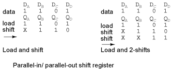
Above, a data pattern is presented to inputs DA DB DC DD. The pattern is loaded to QA QB QC QD . Then it is shifted one bit to the right. The incoming data is indicated by X, meaning the we do no know what it is. If the input (SER) were grounded, for example, we would know what data (0) was shifted in. Also shown, is right shifting by two positions, requiring two clocks.
The above figure serves as a reference for the hardware involved in right shifting of data. It is too simple to even bother with this figure, except for comparison to more complex figures to follow.
Right shifting of data is provided above for reference to the previous right shifter.
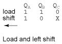
If we need to shift left, the FFs need to be rewired. Compare to the previous right shifter. Also, SI and SO have been reversed. SI shifts to QC. QC shifts to QB. QB shifts to QA. QA leaves on the SO connection, where it could cascade to another shifter SI. This left shift sequence is backwards from the right shift sequence.
Above we shift the same data pattern left by one bit. There is one problem with the "shift left" figure above. There is no market for it. Nobody manufactures a shift-left part. A "real device" which shifts one direction can be wired externally to shift the other direction. Or, should we say there is no left or right in the context of a device which shifts in only one direction. However, there is a market for a device which will shift left or right on command by a control line. Of course, left and right are valid in that context.
What we have above is a hypothetical shift register capable of shifting either direction under the control of L'/R. It is setup with L'/R=1 to shift the normal direction, right. L'/R=1 enables the multiplexer AND gates labeled R. This allows data to follow the path illustrated by the arrows, when a clock is applied. The connection path is the same as the"too simple" "shift right" figure above. Data shifts in at SR, to QA, to QB, to QC, where it leaves at SR cascade. This pin could drive SR of another device to the right. What if we change L'/R to L'/R=0?
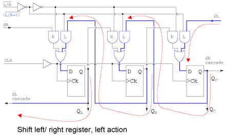
With L'/R=0, the multiplexer AND gates labeled L are enabled, yielding a path, shown by the arrows, the same as the above "shift left" figure. Data shifts in at SL, to QC, to QB, to QA, where it leaves at SL cascade. This pin could drive SL of another device to the left. The prime virtue of the above two figures illustrating the "shift left/ right register" is simplicity. The operation of the left right control L'/R=0 is easy to follow. A commercial part needs the parallel data loading implied by the section title. This appears in the figure below.
Now that we can shift both left and right via L'/R, let us add SH/LD', shift/ load, and the AND gates labeled "load" to provide for parallel loading of data from inputs DA DB DC. When SH/LD'=0, AND gates R and L are disabled, AND gates "load" are enabled to pass data DA DB DC to the FF data inputs. the next clock CLK will clock the data to QA QB QC. As long as the same data is present it will be re-loaded on succeeding clocks. However, data present for only one clock will be lost from the outputs when it is no longer present on the data inputs. One solution is to load the data on one clock, then proceed to shift on the next four clocks. This problem is remedied in the 74ALS299 by the addition of another AND gate to the multiplexer. If SH/LD' is changed to SH/LD'=1, the AND gates labeled "load" are disabled, allowing the left/ right control L'/R to set the direction of shift on the L or R AND gates. Shifting is as in the previous figures. The only thing needed to produce a viable integrated device is to add the fourth AND gate to the multiplexer as alluded for the 74ALS299. This is shown in the next section for that part.
|
|
| Home Digital Shift Registers Parallel-In, Parallel-Out, Universal Shift Register |
|


Last Update: 2010-11-19