| The ebook FEEE - Fundamentals of Electrical Engineering and Electronics is based on material originally written by T.R. Kuphaldt and various co-authors. For more information please read the copyright pages. |

|
Home  Digital Shift Registers Parallel-In, Parallel-Out, Universal Shift Register PIPO Universal Devices Digital Shift Registers Parallel-In, Parallel-Out, Universal Shift Register PIPO Universal Devices |
|


|
  |
|
PIPO Universal DevicesLet's take a closer look at Serial-in/ parallel-out shift registers available as integrated circuits, courtesy of Texas Instruments. For complete device data sheets, follow the links. 395, 74LS395, shift register 299, 74ALS299, shift register
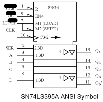
395, 74LS395A ANSI symbol We have already looked at the internal details of the SN74LS395A, see above previous figure, 74LS395 parallel-in/ parallel-out shift register with tri-state output. Directly above is the ANSI symbol for the 74LS395. Why only 4-bits, as indicated by SRG4 above? Having both parallel inputs, and parallel outputs, in addition to control and power pins, does not allow for any more I/O (Input/Output) bits in a 16-pin DIP (Dual Inline Package). R indicates that the shift register stages are reset by input CLR' (active low- inverting half arrow at input) of the control section at the top of the symbol. OC', when low, (invert arrow again) will enable (EN4) the four tristate output buffers (QA QB QC QD ) in the data section. Load/shift' (LD/SH') at pin (7) corresponds to internals M1 (load) and M2 (shift). Look for prefixes of 1 and 2 in the rest of the symbol to ascertain what is controlled by these. The negative edge sensitive clock (indicated by the invert arrow at pin-10) C3/2has two functions. First, the 3 of C3/2 affects any input having a prefix of 3, say 2,3D or 1,3D in the data section. This would be parallel load at A, B, C, D attributed to M1 and C3 for 1,3D. Second, 2 of C3/2-right-arrow indicates data clocking wherever 2 appears in a prefix (2,3D at pin-2). Thus we have clocking of data at SER into QA with mode 2 . The right arrow after C3/2 accounts for shifting at internal shift register stages QA QB QC QD. The right pointing triangles indicate buffering; the inverted triangle indicates tri-state, controlled by the EN4. Note, all the 4s in the symbol associated with the EN are frequently omitted. Stages QB QC are understood to have the same attributes as QD. QD' cascades to the next package's SER to the right.
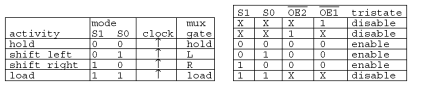
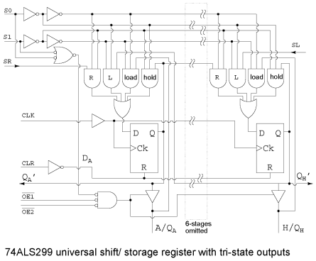
bus, shift register 299, 74LS299 The table above, condensed from the data '299 data sheet, summarizes the operation of the 74ALS299 universal shift/ storage register. Follow the '299 link above for full details. The Multiplexer gates R, L, load operate as in the previous "shift left/ right register" figures. The difference is that the mode inputs S1 and S0 select shift left, shift right, and load with mode set to S1 S0 = to 01, 10, and 11respectively as shown in the table, enabling multiplexer gates L, R, and load respectively. See table. A minor difference is the parallel load path from the tri-state outputs. Actually the tri-state buffers are (must be) disabled by S1 S0 = 11 to float the I/O bus for use as inputs. A bus is a collection of similar signals. The inputs are applied to A, B through H (same pins as QA, QB, through QH) and routed to the load gate in the multiplexers, and on the the D inputs of the FFs. Data is parallel load on a clock pulse. The one new multiplexer gate is the AND gate labeled hold, enabled by S1 S0 = 00. The hold gate enables a path from the Q output of the FF back to the hold gate, to the D input of the same FF. The result is that with mode S1 S0 = 00, the output is continuously re-loaded with each new clock pulse. Thus, data is held. This is summarized in the table. To read data from outputs QA, QB, through QH, the tri-state buffers must be enabled by OE2', OE1' =00 and mode =S1 S0 = 00, 01, or 10. That is, mode is anything except load. See second table.
Right shift data from a package to the left, shifts in on the SR input. Any data shifted out to the right from stage QH cascades to the right via QH'. This output is unaffected by the tri-state buffers. The shift right sequence for S1 S0 = 10 is:
SR > QA > QB > QC > QD > QE > QF > QG > QH (QH')
Left shift data from a package to the right shifts in on the SL input. Any data shifted out to the left from stage QA cascades to the left via QA', also unaffected by the tri-state buffers. The shift left sequence for S1 S0 = 01 is:
(QA') QA < QB < QC < QD < QE < QF < QG < QH (QSL')
Shifting may take place with the tri-state buffers disabled by one of OE2' or OE1' = 1. Though, the register contents outputs will not be accessible. See table.
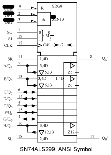
299, 74LS299 ANSI symbol The "clean" ANSI symbol for the SN74ALS299 parallel-in/ parallel-out 8-bit universal shift register with tri-state output is shown for reference above.
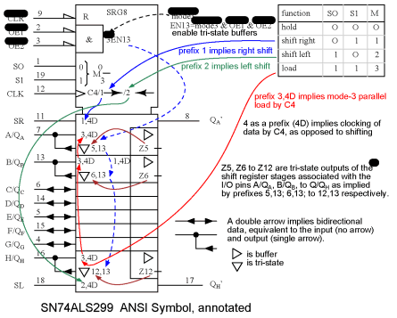
The annotated version of the ANSI symbol is shown to clarify the terminology contained therein. Note that the ANSI mode (S0 S1) is reversed from the order (S1 S0) used in the previous table. That reverses the decimal mode numbers (1 & 2). In any event, we are in complete agreement with the official data sheet, copying this inconsistency.
|
|
| Home Digital Shift Registers Parallel-In, Parallel-Out, Universal Shift Register PIPO Universal Devices |
|
Last Update: 2010-11-19