| The ebook FEEE - Fundamentals of Electrical Engineering and Electronics is based on material originally written by T.R. Kuphaldt and various co-authors. For more information please read the copyright pages. |

|
Home  Semiconductors Solid-State Device Theory Crystal Structure Semiconductors Solid-State Device Theory Crystal Structure |
|


|
  |
|
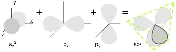
Crystal StructureMost inorganic substances form their atoms (or ions) into an ordered array known as a crystal. The outer electron clouds of atoms interact in an orderly manner. Even metals are composed of crystals at the microscopic level. If a metal sample is given an optical polish, then acid etched, the microscopic microcrystalline structure shows as in Figure below. It is also possible to purchase, at considerable expense, metallic single crystal specimens from specialized suppliers. Polishing and etching such a specimen discloses no microcrystalline structure. Practically all industrial metals are polycrystalline. Most modern semiconductors, on the other hand, are single crystal devices. We are primarily interested in monocrystalline structures. (a) Metal sample, (b) polished, (c) acid etched to show microcrystalline structure. Many metals are soft and easily deformed by the various metal working techniques. The microcrystals are deformed in metal working. Also, the valence electrons are free to move about the crystal lattice, and from crystal to crystal. The valence electrons do not belong to any particular atom, but to all atoms. The rigid crystal structure in Figure below is composed of a regular repeating pattern of positive Na ions and negative Cl ions. Once the Na and Cl atoms have formed Na+ and Cl- ions by transferring an electron from Na to Cl, with no free electrons. Electrons are not free to move about the crystal lattice, a difference compared with a metal. Nor are the ions free. Ions are fixed in place within the crystal structure. Though, the ions are free to move about if the NaCl crystal is dissolved in water. However, the crystal no longer exists. The regular, repeating structure is gone. Evaporation of the water deposits the Na+ and Cl- ions in the form of new crystals as the oppositely charged ions attract each other. Ionic materials form crystal structures due to the strong electrostatic attraction of the oppositely charged ions. NaCl crystal having a cubic structure. Semiconductors in Group IV also form crystals because of the tetrahedral bonding pattern of the s2p2 electrons about the atom, sharing electron-pair bonds to four adjacent atoms. (Figure below(a) ) More correctly the four outer electrons: two in the s-orbital, (sz) offset along the z-axis, and two in the p-orbital (px and py) hybridize to form four sp3 molecular orbitals. These four electron clouds repell one another to equidistant tetrahedral spacing about the Si atom, attracted by the positive nucleus as shown in Figure below. Two s-orbital (sz ) electrons and two p-orbital (sx and sy ) electrons hybridize, (c) forming four sp3 molecular orbitals. Every semiconductor atom, Si, Ge, or C (diamond) is chemically bonded to four other atoms by covalent bonds, shared electron bonds. Two electrons may share an orbital if each have opposite spin quantum numbers. Thus, an unpaired electron may share an orbital with an electron from another atom. This corresponds to overlapping Figure below(a) of the electron clouds, or bonding. Figure below (b) is one fourth of the volume of the diamond crystal structure unit cell shown in Figure below at the origin. The bonds are particularly strong in diamond, decreasing in strength going down group IV to silicon, and germanium. Silicon and germanium both form crystals with a diamond structure. (a) Tetrahedral bonding of Si atom. (b) leads to 1/4 of the cubic unit cell The diamond unit cell, the basic crystal building block, in Figure below shows four atoms (dark) bonded to four others within the volume of the cell. This is equivalent to placing one of Figure above(b) at the origin in Figure below, then placing three more on adjacent faces to fill the full cube. Six atoms fall on the middle of each of the six cube faces, showing two bonds. The other two bonds to adjacent cubes were omitted for clarity. Out of eight cube corners, four atoms bond to an atom within the cube. Where are the other four atoms bonded? The other four bond to adjacent cubes of the crystal. Keep in mind that even though four corner atoms show no bonds in the cube, all atoms within the crystal are bonded in one giant molecule. A semiconductor crystal is built up from copies of this unit cell. Si, Ge, and C (diamond) form interleaved face centered cube. The crystal is effectively one molecule. An atom covalent bonds to four others, which in turn bond to four others, and so on. The crystal lattice is relatively stiff resisting deformation. Few electrons free themselves for conduction about the crystal. A property of semiconductors is that once an electron is freed, a positively charged empty space develops which also contributes to conduction.
|
|
| Home Semiconductors Solid-State Device Theory Crystal Structure |
|


Last Update: 2010-11-19