| The ebook FEEE - Fundamentals of Electrical Engineering and Electronics is based on material originally written by T.R. Kuphaldt and various co-authors. For more information please read the copyright pages. |

|
Home  Semiconductors Solid-State Device Theory Quantum Devices Magnetic Tunnel Junction Semiconductors Solid-State Device Theory Quantum Devices Magnetic Tunnel Junction |
||||||


|
  |
|||||
|
Magnetic Tunnel Junction
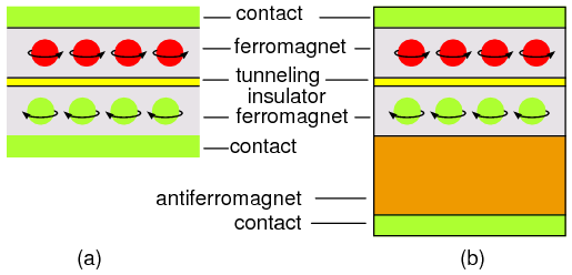
A simple magnetic tunnel junction (MTJ) is shown in Figure 3435(a), consisting of a pair of ferromagnetic, strong magnetic properties like iron (Fe), layers separated by a thin insulator. Electrons can tunnel through a sufficiently thin insulator due to the quantum mechanical properties of electrons-- the wave nature of electrons. The current flow through the MTJ is a function of the magnetization, spin polarity, of the ferromagnetic layers. The resistance of the MTJ is low if the magnetic spin of the top layer is in the same direction (polarity) as the bottom layer. If the magnetic spins of the two layers oppose, the resistance is higher.
The change in resistance can be enhanced by the addition of an antiferromagnet, material having spins aligned but opposing, below the bottom layer in Figure 3435 (b). This bias magnet pins the lower ferromagnetic layer spin to a single unchanging polarity. The top layer magnetization (spin) may be flipped to represent data by the application of an external magnetic field not shown in the figure. The pinned layer is not affected by external magnetic fields. Again, the MTJ resistance is lowest when the spin of the top ferromagnetic layer is the same sense as the bottom pinned ferromagnetic layer.
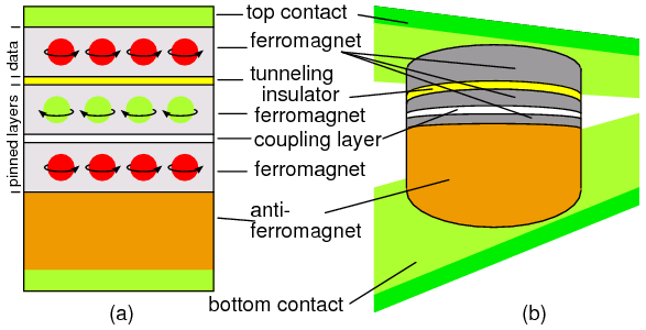
The MTJ may be improved further by splitting the pinned ferromagnetic layer into two layers separated by a buffer layer in Figure 3434 (a). This isolates the top layer. The bottom ferromagnetic layer is pinned by the antiferromagnet as in the previous figure. The ferromagnetic layer atop the buffer is attracted by the bottom ferromagnetic layer. Opposites attract. Thus, the spin polarity of the additional layer is opposite of that in the bottom layer due to attraction. The bottom and middle ferromagnetic layers remain fixed. The top ferromagnetic layer may be set to either spin polarity by high currents in proximate conductors (not shown). This is how data are stored. Data are read out by the difference in current flow through the tunnel junction. Resistance is lowest if the layers on both sides of the insulting layer are of the same spin.
An array of magnetic tunnel junctions may be embedded in a silicon wafer with conductors connecting the top and bottom terminals for reading data bits from the MTJ's with conventional CMOS circuitry. One such MTJ is shown in Figure 3434 (b) with the read conductors. Not shown, another crossed array of conductors carrying heavy write currents switch the magnetic spin of the top ferromagnetic layer to store data. A current is applied to one of many “X” conductors and a “Y” conductor. One MTJ in the array is magnetized under the conductors' cross-over. Data are read out by sensing the MTJ current with conventional silicon semiconductor circuitry.

Not a commercial product, or even a laboratory device, is the theoretical spin transistor which might one day make spin logic gates possible. The spin transistor is a derivative of the theoretical spin diode.
It has been known for some time that electrons flowing through a cobalt-iron ferromagnet become spin polarized. The ferromagnet acts as a filter passing electrons of one spin preferentially. These electrons may flow into an adjacent nonmagnetic conductor (or semiconductor) retaining the spin polarization for a short time, nano-seconds. Though, spin polarized electrons may propagate a considerable distance compared with semiconductor dimensions. The spin polarized electrons may be detected by a nickel-iron ferromagnetic layer adjacent to the semiconductor.
It has also been shown that electron spin polarization occurs when circularly polarized light illuminates some semiconductor materials. Thus, it should be possible to inject spin polarized electrons into a semiconductor diode or transistor. The interest in spin based transistors and gates is because of the non-dissipative nature of spin propagation, compared with dissipative charge flow. As conventional semiconductors are scaled down in size, power dissipation increases. At some point the scaling down will no longer be practical. Researchers are looking for a replacement for the conventional charge flow based transistor. That device may be based on spintronics.
|
||||||
| Home Semiconductors Solid-State Device Theory Quantum Devices Magnetic Tunnel Junction |
|
|||||
Last Update: 2010-11-19