| Transistor Basics is a free introductory textbook on transistors and their basic applications. See the editorial for more information.... |

|
Home  The Grounded Base Transistor Four-Terminal Analysis of Transistors Measuring Circuits The Grounded Base Transistor Four-Terminal Analysis of Transistors Measuring Circuits |
||
| See also: Basic Circuits | ||


|
  |
|
|
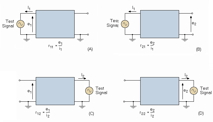
Measuring CircuitsAuthor: Leonard Krugman Figure 3-8 illustrates the four basic circuits for measuring four-terminal parameters. The double subscript designations on the general resistance parameters of the four-terminal network (those designated r11, r12, r21, and r22) refer to the input terminal 1 and the output terminal 2. In addition, the first subscript refers to the voltage, and the second subscript refers to the current. For example, r12 is the ratio of the input voltage to the output current, while r21 is the ratio of the output voltage to the input current. These designations also indicate whether a test signal is applied to the input or output terminals, since the current will always be measured at the terminals where the test signal is applied.
Fig. 3-8. Basic circuits for measuring four-terminal parameters. There are several sources of error inherent in this use of small-signal inputs to evaluate the parameters of a transistor. The first error is due to the non-linearity of the characteristic curves. The larger the signal input, the greater the error. Thus, to make this error negligible, the signal must be held sufficiently small. In the practical case, the minimum useful signal is limited by the transistor thermal noise.
The third source of error, when small signal inputs are assumed, results from the shunting action of the input voltmeter and the input d-c bias supply on the input signal. The first effect may be made negligible by using a very high resistance voltmeter. The magnitude of the error caused by the shunting action of the d-c bias supply is proportional to the ratio of the transistor input resistance and the d-c supply resistance. Errors are also introduced by the capacities between emitter and base, and between collector and base. These capacitance effects are comparable to the plate to grid and cathode to grid capacitances in a vacuum tube. In the audio frequency range, these errors are generally neglected.
|
||
| Home The Grounded Base Transistor Four-Terminal Analysis of Transistors Measuring Circuits |
|
|
Last Update: 2007-07-12