| Transistor Basics is a free introductory textbook on transistors and their basic applications. See the editorial for more information.... |

|
Home  The Grounded Base Transistor The Grounded Base Connection Power Gain The Grounded Base Transistor The Grounded Base Connection Power Gain |
|||||||||||||||||||||||||||||


|
  |
||||||||||||||||||||||||||||
|
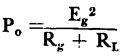
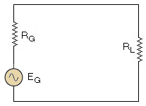
Power GainAuthor: Leonard Krugman Before determining the power gain included in transistor circuits, some definitions must be considered. Figure 3-16 illustrates a signal generator Eg with an internal resistance Rg feeding into a load RL. The total power delivered by the generator
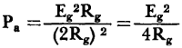
Fig. 3-16. Simplified transistor equivalent circuit for analysis of power gain. By using conventional calculus methods for determining conditions for maximum power, it is found that the load power is maximum when Rg = RL. Under this condition the power available from the generator
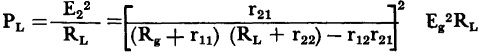
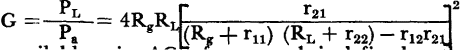
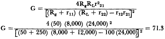
The operating gain, G, of a network is defined as the ratio of the power dissipated in the load to the power available from the generator. For the general transistor circuit of Fig. 3-9
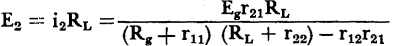
The power dissipated in the load
The operating gain
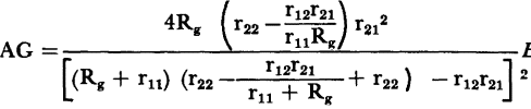
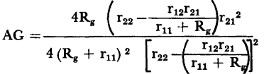
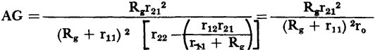
The available gain, AG, of a network is defined as tne ratio of the power dissipated in the load to the power available from the generator when the load is matched to the output resistance. When RL = ro = Substituting in equation 3-46, the available gain
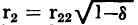
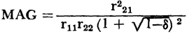
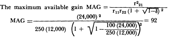
The maximum available gain, MAG, of a network is defined as the ratio of the power dissipated in the load to the power available from the generator when the generator internal resistance is matched to the input transistor resistance, and when the load resistance is matched to the transistor output resistance. In order to solve for the maximum power gain in terms of the open-circuit parameters, the image-matched input and output resistances, previously determined, are substituted in the operating gain equation 3-46. Then, the maximum available gain,
where
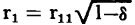
and
Substituting: equations 3-37 and 3-41 in equation 3-50, for r1 and r2,
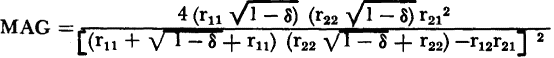
from which derives
For the typical point-contact transistor, when r11 = 250 ohms, r12 =100 ohms, r21 = 24,000 ohms, r22 = 12,000 ohms, and when assuming Rg = 50 ohms and RL = 8,000 ohms, the operating gain G, becomes
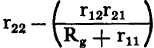
Notice that the stability factor,
From equation (3-55)
|
|||||||||||||||||||||||||||||
| Home The Grounded Base Transistor The Grounded Base Connection Power Gain |
|
||||||||||||||||||||||||||||
 ; the power dissipated in the load
  . Since
  then
then 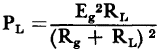 .
.
 , then
 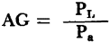 .
. 

 .
.


 , is
, is 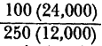 = 0.8. If the stability factor is greater than one, the numerical value of the quantity
  must be negative, which indicates an unstable condition. For the typical junction transistor in which r11 = 550 ohms, r12 = 500 ohms, r21 = 1,900,000 ohms, and r22 = 2,000,000 ohms; when assuming Rg = 100 ohms and RL = 1,000,000 ohms, the operating gain

Last Update: 2007-07-12