| Transistor Basics is a free introductory textbook on transistors and their basic applications. See the editorial for more information.... |
|
Home  Grounded Emitter and Grounded Collector Transistors The Grounded Emitter Connection Power Gain Grounded Emitter and Grounded Collector Transistors The Grounded Emitter Connection Power Gain |
||


|
  |
|
|
Power Gain in the Grounded Emitter ConnectionAuthor: Leonard Krugman The numerical values of the voltage and current gains are always negative in the stable range of operation of the grounded emitter connection. The negative sign is merely a mathematical indication of the phase inversion of the amplified signal. Since the power gain is a function of the product of the voltage and current gains, its numerical value must be positive. The operating gain is defined in equation 3-46 as
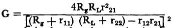
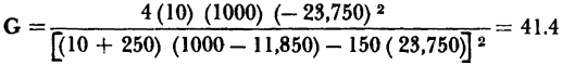
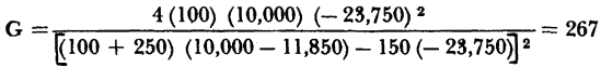
However, Fig. 4-3 indicates that at a load of RL = 1,000 ohms, the transistor is unstable and will oscillate. This does not mean that the grounded emitter connected transistor can oscillate and supply a power gain at the same time, but rather that the operating gain equation can only be applied conditionally. Without going too deeply into the mathematical concepts involved, equation 3-46 can only be applied when (Rg + r11) (RL + r22) - r12r21 is greater than zero. When Rg and RL equal zero, the worst possible case, the condition equation becomes r11r12 — r12r21 > 0. This is just another way of expressing the requirement that the stability factor, ë = In the typical point-contact transistor under discussion, ë = 1.19, the conditional equation is (Rg + 250) (RL - 11,850) - 150 (- 23,750) > 0. A plot of this conditional characteristic is shown in Fig. 4-7. Any combination of generator resistance and load resistance in the stable region can be used, but the selection of operating values close to the conditional characteristic provides the greatest operating gain.
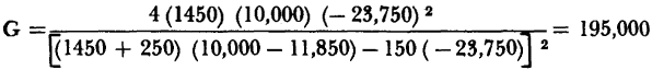
Fig. 4-7. Conditional stability characteristic (grounded emitter). The following example illustrates the design of a grounded emitter circuit for maximum power gain when the stability factor is greater than one. Assume that the load RL is fixed at 10,000 ohms for the typical point-contact transistor. Figure 4-7 indicates than any value of Kg less than 1,530 ohms will provide stable operation. Thus for Rg = 100 ohms
If, however, Kg = 1,450 ohms were selected,
These examples prove that extremely high values of power gain can be attained by selection of RgRL values close to the stability characteristic. In the practical case, however, the selected values must be sufficiently removed from the instability limit to avoid the introduction of circuit oscillation by normal parameter variations. The grounded emitter connection can be stabilized by adding resistance in the emitter arm. As an example, assume that a resistor Re = 850 ohms is added in series with the emitter. The four-terminal parameters then become:
Substituting these new values, the conditional equation becomes (Rg + 1,100) (RL— 11,000) -(1,000) (-22,900) and must be greater than zero. A plot of the modified conditional stability characteristic is shown in Fig. 4-7. Notice the extent to which the stability area has been increased. As before, the selection of values RL and Rg located near the limiting line provide the greatest power gain.
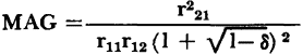
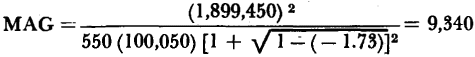
The maximum available power gain defined by equation 3-55, can be applied to thegrounded emitter connection provided that the stability factor is less than one. The numerical value of the maximum available gain for the typical junction transistor is:
|
||
| Home Grounded Emitter and Grounded Collector Transistors The Grounded Emitter Connection Power Gain |
|
|
 , must be less than unity. As a result, the operating gain is conditional when ë is greater than unity.
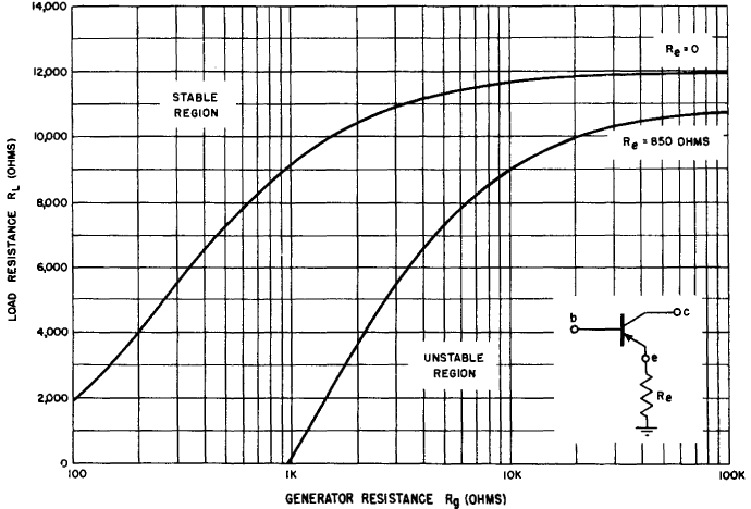
Last Update: 2010-11-17