| Transistor Basics is a free introductory textbook on transistors and their basic applications. See the editorial for more information.... |

|
Home  Transistor Amplifiers Class A Amplifiers Maximum Output Conditions Transistor Amplifiers Class A Amplifiers Maximum Output Conditions |
||


|
  |
|
|
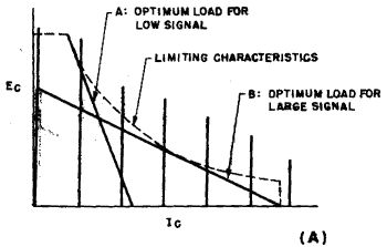
Maximum Output ConditionsAuthor: Leonard Krugman Since the power handling capacity of the transistor is small compared to that of the vacuum tube, it is usually necessary to drive the transistor to its maximum limits. When a transistor amplifier is designed for maximum power, as in Fig. 5-10 (C), it is properly termed a power amplifier, although the actual power involved may only amount to a hundred milliwatts. To obtain maximum power, the load line is selected to include the maximum possible area concurrent with the fixed limitations of maximum collector dissipation, current, and voltage. The ideal load for maximum power would be one which followed exactly the transistor limit boundaries illustrated in Fig. 5-1.
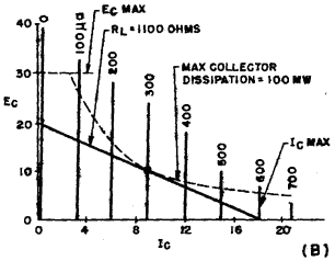
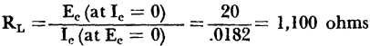
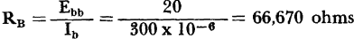
Fig. 5-10. (A) Load fines for maximum power. (B) Determination of optimum load. (C) Power amplifier circuit. The calculations for determining the conditions for maximum output in a power amplifier stage, assuming a transistor with the characteristics illustrated in Fig. 5-10 (B), are as follows: Assume a battery supply Ebb = 20 volts. This determines a point on the load line for Ic = 0. Now hold one end of a straight edge on this point and swing the edge until it just touches a point on the maximum collector dissipation line. Draw a line through the two points. This is the optimum load line for the given conditions. The maximum input signal, the d-c bias resistors, and the distortion can all be computed directly from the figure by means of the methods discussed in the preceding paragraphs:
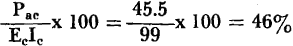
Using the standard equation derived for vacuum-tube circuits, the transistor a-c output Pac is one-eighth of the product of the peak-to-peak collector voltage and collector current:
Since the maximum d-c power is EcIc = 11 × 9× 10-3 = 99 milliwatts, the efficiency becomes
The maximum a-c signal current can be taken directly from the characteristic curve. In this case, ib = 600 μa peak-to-peak. (The stabilizing resistors have been omitted to simplify the illustration.)
|
||
| Home Transistor Amplifiers Class A Amplifiers Maximum Output Conditions |
|
|


Last Update: 2010-11-17