|
Typical Circuit
Author: Leonard Krugman
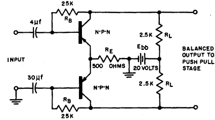
Fig. 5-14. Transistor phase inverter.
Figure 5-14 illustrates the basic circuit of a transistor phase inverter, which provides a reasonably well-balanced output. The basic operation is as follows: the upper transistor operates as a conventional grounded emitter amplifier except that the emitter is grounded through the parallel circuit, consisting of the lower transistor emitter-base path and resistor RE.
The emitter-base path has a low resistance, less than 50 ohms, so that practically all of the a-c emitter current of the top transistor flows through this path. Since the emitter current value for each transistor is the same, the collector currents are also equal if the current gains from emitter to collector are equal. For proper operation, the load resistances should be small compared to the output resistances of the transistors, and the emitter-to-collector current gains should be well matched. For the circuit illustrated, the output resistance of each transistor is the collector resistance shunted by RB. Since rc is much greater than RB, the output resistance is equal to RB. Thus RB should be about ten times RL. It is not necessary for the current gains to be exactly matched. Values which fall in the range of .92 to .97 are usually satisfactory. RL and RB are selected to provide the operating biases, which in this case are Ec = 10 volts, Ic = 4 ma, and Ib = 400 μa. The value of RE is particularly important. It must be large compared to the emitter-to-base resistance path of the lower transistor; if it is not, an appreciable portion of the a-c signal will be shunted through RE and the currents in the emitters will not be equal. In general, a value of RE that is ten times the emitter-to-base circuit resistance is satisfactory.
|

 Transistor Amplifiers


