| Transistor Basics is a free introductory textbook on transistors and their basic applications. See the editorial for more information.... |

|
Home  Transistor High Frequency Applications Printed Circuit Techniques Transistor High Frequency Applications Printed Circuit Techniques |
||


|
  |
|
|
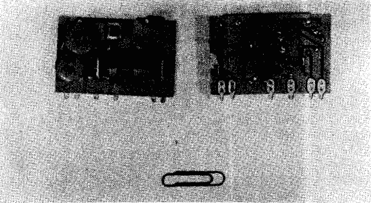
Printed Circuit TechniquesAuthor: Leonard Krugman One of the most promising features of the transistor is its ability to fit into the new prefabricated wiring techniques, by which the maze of hand-soldered wires normally associated with electronic equipment has been eliminated. Basically, a printed circuit starts with a metal foil bonded to one or both sides of an insulating plastic material. The metal foil may be copper (most popular) aluminum, silver, or brass. Most types of laminated plastics are suitable as the base insulator. The circuit is drawn on the foil clad laminate with an acid resistant ink. The complete assembly is then dipped into an etching solution which removes the metal not protected by ink. Holes are then drilled or punched into the assembly at appropriate points, and into these holes the various circuit components are inserted and soldered to the metal foil. If the circuit is at all complex, hand soldering is extremely tedious and difficult, and the dip soldering technique is used. In this method, components with preformed leads are inserted into the holes, either manually or by an automatic process. After fluxing, all the connections between the component leads and the circuit pattern are accomplished by a "one-shot" dip in a molten solder bath. Those portions of the circuit which must be left free of the solder are coated with a protective lacquer or masked before the solder bath. Dip soldering assures very reliable solder joints in one simple operation, and also permits a greater reduction in size by means of stacking techniques, which were previously limited by the space requirements for hand soldering operations. which may be soldered and unsoldered several times during the life of the equipment. Repeated soldering at the foil will eventually cause it to lift from the plastic base. In spite of the small cross-sectional area of the foil conductors, the current carrying capacity of the printed circuit is good, due to the relatively large surface area and the heat conduction by the base material. A 1/32-inch copper foil conductor, for example, can safely handle about five amperes. Increased temperatures caused by current overloads causes the metallic conductor to buckle and separate from the base. One of the major advantages of the printed circuit is its uniformity from unit to unit. For example, the distributed capacitance between foil conductors is in the same order of magnitude as that of a carefully hand wired assembly. In the prefabricated type, however, the value remains constant from unit to unit because they are all produced from the same master design. Figure 7-11 illustrates the front and back of an experimental printed circuit type of transistor if amplifier. The component arrangement can be seen at the left of the illustration and the printed wiring can be seen at the right. Miniature components for use with transistors are shown in Fig. 7-12. The top row of the figure shows a miniaturized transformer and three resistors. The bottom row illustrates an inductor, a capacitor, two junction transistor sockets, and two point-contact transistor sockets.
Fig. 7-11. Experimental transistor i-f amplifier. The marriage of standard and miniaturized components with the basic printed circuit is, in essence, the "autosembly" technique devised by the Signal Corps Engineering Laboratories. This method is best suited to present production facilities, since it utilized components with proven reliability. However, the recent progress in the development of printed components indicates that most of the applications of prefabricated circuits are still to come. Printed resistors having values of 10 ohms to 10 megs and which are sprayed onto an area of 1/16 of a square inch have been used successfully. Small inductance coils, having values up to 20
Fig. 702. Miniature transistor components. The transistor, because of its mechanical ruggedness and long life expectancy, is well adapted for direct assembly into printed circuit patterns. The minute heat generated by the transistor makes its future use in compact packaged equipment particularly promising. The prefabrication techniques will initially reduce the out-of-service time considerably, since complete circuits will be encapsulated in units no larger than present vacuum tubes. On the other hand, assembly repairs will require great skill and technical knowledge due to the complex arrangement of the miniaturized components.
|
||
| Home Transistor High Frequency Applications Printed Circuit Techniques |
|
|
 H, can be etched into the printed circuit, and capacitors ranging from 10 pF to 1 nF can be incorporated in the printed circuit by etching opposite sides of foil-clad glass-cloth laminates.
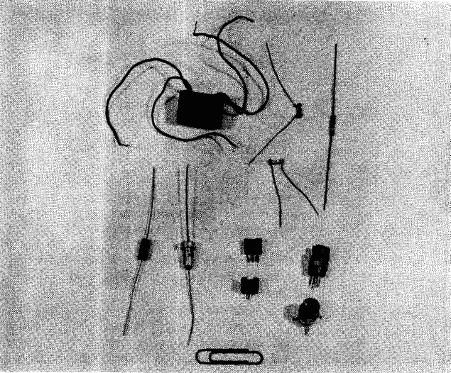
Last Update: 2010-11-17