| The ebook FEEE - Fundamentals of Electrical Engineering and Electronics is based on material originally written by T.R. Kuphaldt and various co-authors. For more information please read the copyright pages. |

|
Home  Digital Shift Registers Parallel-In, Parallel-Out, Universal Shift Register Practical Applications Digital Shift Registers Parallel-In, Parallel-Out, Universal Shift Register Practical Applications |
|


|
  |
|
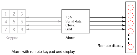
PIPO Practical ApplicationsThe Alarm with remote keypad block diagram is repeated below. Previously, we built the keypad reader and the remote display as separate units. Now we will combine both the keypad and display into a single unit using a universal shift register. Though separate in the diagram, the Keypad and Display are both contained within the same remote enclosure.
We will parallel load the keyboard data into the shift register on a single clock pulse, then shift it out to the main alarm box. At the same time , we will shift LED data from the main alarm to the remote shift register to illuminate the LEDs. We will be simultaneously shifting keyboard data out and LED data into the shift register.
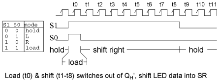
Eight LEDs and current limiting resistors are connected to the eight I/O pins of the 74ALS299 universal shift register. The LEDS can only be driven during Mode 3 with S1=0 S0=0. The OE1' and OE2' tristate enables are grounded to permenantly enable the tristate outputs during modes 0, 1, 2. That will cause the LEDS to light (flicker) during shifting. If this were a problem the EN1' and EN2' could be ungrounded and paralleled with S1 and S0 respectively to only enable the tristate buffers and light the LEDS during hold, mode 3. Let's keep it simple for this example. During parallel loading, S0=1 inverted to a 0, enables the octal tristate buffers to ground the switch wipers. The upper, open, switch contacts are pulled up to logic high by the resister-LED combination at the eight inputs. Any switch closure will short the input low. We parallel load the switch data into the '299 at clock t0 when both S0 and S1 are high. See waveforms below.
Once S0 goes low, eight clocks (t0 tot8) shift switch closure data out of the '299 via the Qh' pin. At the same time, new LED data is shifted in at SR of the 299 by the same eight clocks. The LED data replaces the switch closure data as shifting proceeds. After the 8th shift clock, t8, S1 goes low to yield hold mode (S1 S0 = 00). The data in the shift register remains the same even if there are more clocks, for example, T9, t10, etc. Where do the waveforms come from? They could be generated by a microprocessor if the clock rate were not over 100 kHz, in which case, it would be inconvenient to generate any clocks after t8. If the clock was in the megahertz range, the clock would run continuously. The clock, S1 and S0 would be generated by digital logic, not shown here.
|
|
| Home Digital Shift Registers Parallel-In, Parallel-Out, Universal Shift Register Practical Applications |
|

Last Update: 2010-11-19