| Transistor Basics is a free introductory textbook on transistors and their basic applications. See the editorial for more information.... |

|
Home  The Grounded Base Transistor The Grounded Base Connection Input and Output Impedance Matching The Grounded Base Transistor The Grounded Base Connection Input and Output Impedance Matching |
||||||||||||||||||||||||||||||||||||


|
  |
|||||||||||||||||||||||||||||||||||
|
Input and Output Impedance MatchingAuthor: Leonard Krugman Equations 3-13 and 3-21 indicate that the input resistance is affected by the load resistance and, conversely, the output resistance depends on the generator internal resistance.
Solving in terms of r12r21
Substituting for Rg and ro in equation 3-21
Again solving in terms of r12r21
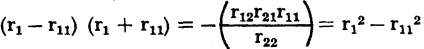
Equating equations 3-27 and 3-29
Cross multiplying and cancelling equal terms,
or
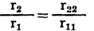
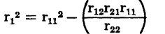
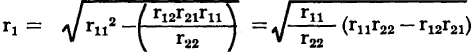
This latter equation indicates that matching the input and output resistances for maximum power gain requires their values to be in the same ratio as the open-circuit characteristics of the transistor. The absolute value of the generator internal resistance and its matched input resistance in terms of transistor open-circuit parameters can now be determined. Substituting the equality
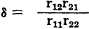
In terms of the stability factor,
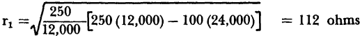
For the typical point-contact transistor previously considered, when r11 = 250 ohms, r12 = 100 ohms, r21 = 24,000 ohms, and r22 = 12,000 ohms, the numerical value of r1 is
For the typical junction transistor, when r11 = 550 ohms, r12 = 500 ohms, r21 = 1,900,000 ohms, and r22 = 2,000,000 ohms,
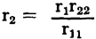
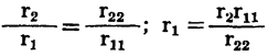
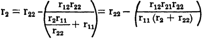
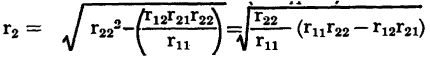
The output image resistance of a transistor can be determined in a similar fashion from the ratio
Substituting this equality into equation 3-28
In terms of the stability factor
For the typical point-contact transistor,
Forthe typical junction transistor
These values may be checked on the RL vs ri and Rg vs ro characteristics plotted for these typical transistors in Figs. 3-11, 3-12, 3-14, and 3-15.
|
||||||||||||||||||||||||||||||||||||
| Home The Grounded Base Transistor The Grounded Base Connection Input and Output Impedance Matching |
|
|||||||||||||||||||||||||||||||||||

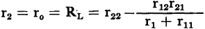
 into equation 3-26,
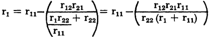
 , which will be defined later in the chapter, the input image resistance
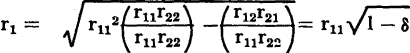


 ; the output image resistance


Last Update: 2010-11-17