| Transistor Basics is a free introductory textbook on transistors and their basic applications. See the editorial for more information.... |
|
Home  Grounded Emitter and Grounded Collector Transistors The Grounded Collector Connection Output Resistance Grounded Emitter and Grounded Collector Transistors The Grounded Collector Connection Output Resistance |
||||


|
  |
|||
|
Output Resistance for the Grounded Collector ConnectionAuthor: Leonard Krugman The output resistance is defined by equation 3-21:
In terms of the internaltransistor parameters, the output resistance becomes:
Fig. 4-12. Output resistance vs generator resistance for typical point-contact transistor (grounded collector).
Fig. 4-13. Output resistance vs generator resistance for typical junction transistor. As in the case of the grounded emitter, the grounded collector circuit using the point-contact transistor cannot be matched on an image basis without external modification, since the stability factor of this circuit is greater than one. However, the grounded collector does exhibit a unique characteristic when external resistance is added in the collector arm. For example, assume that a resistor Rc is added to the collector arm so that Rc + rc = rm. For this modification,
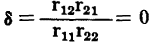
Since r12 = 0, the stability factor
and the output image matched resistance (equation 3-41) becomes
Notice also that ri = r1 = r11 and ro = r2 = r22. Thus, adding a suitable external resistor in the collector arm causes the circuit to act as a perfect buffer stage in which both the input and output resistances are independent of RL and Rg. Numerical values for the typical point-contact transistor modified to act as a buffer stage are:
The image matched input and output equations can be applied to the junction transistor since its stability factor is always slightly less than one. A practical method to use in selecting values to be substituted in these equations indicates that r1 should be chosen to equal 2 percent of r11, and r2 equal to 2 percent of r22. The exact determination of the linage matched resistances in the grounded collector circuit is not important, because the power gain is constant over a wide range of load resistances when the signal generator is matched to the input resistance. In the junction transistor, numerical values for image matched resistances are If the approximate values are used
|
||||
| Home Grounded Emitter and Grounded Collector Transistors The Grounded Collector Connection Output Resistance |
|
|||


 .Thus, the modified circuit is stable. The input image matched resistance (equation 3-37) is then


Last Update: 2010-11-17